
Heracles: A Technical Deep Dive
Intel's Heracles is a purpose-built 197 mm² PCIe accelerator fabricated on Intel 3, featuring an 8192-way SIMD engine with 64 tile-pairs in an 8×8 mesh, 48 GB HBM3, and dedicated NTT/INTT hardware that delivers 1,074× to 5,547× speedup over a 24-core Sapphire Rapids Xeon on core FHE operations while running at 1.2 GHz within a 176 W envelope.
Executive Summary
- Heracles is Intel’s first silicon implementation of a fully homomorphic encryption (FHE) accelerator, designed exclusively to perform arithmetic directly on encrypted data without decryption, supporting BGV, BFV, and CKKS schemes.
- The chip achieves 1,074×–5,547× performance gains versus a 24-core Intel Xeon W7-3455 (Sapphire Rapids) across seven representative FHE primitives, with a key Number Theoretic Transform (NTT) completing in 39 μs (2,355× faster).
- Architecture centers on an 8192-lane 32-bit SIMD datapath, 64 tile-pairs arranged in an 8×8 mesh, 48 GB HBM3, 64 MB on-chip scratchpad, and specialized butterfly units, delivering up to 29.5 TOPS for butterfly operations and multi-terabit/s transform throughput.
- Fabricated on Intel 3 at 197 mm² and 176 W TDP, Heracles is currently a liquid-cooled PCIe card, marking the first practical step toward commercial FHE acceleration for privacy-preserving cloud, ML, and database workloads.
Technical Architecture
Fully homomorphic encryption enables arbitrary computation on ciphertexts such that decrypting the result yields the same output as operating on the plaintext. The primary barriers have been enormous integer sizes (often thousands of bits), frequent Number Theoretic Transforms (NTT), inverse NTTs, automorphisms, and periodic bootstrapping to manage noise growth. General-purpose CPUs and GPUs handle these workloads poorly due to insufficient parallelism, awkward data movement patterns, and lack of native support for modular arithmetic at scale.
Heracles addresses these with a domain-specific architecture. At its core is an 8192-way SIMD compute engine built from 64 tile-pairs organized in an 8×8 mesh network-on-chip. Each tile-pair contains 128 parallel arithmetic lanes, and each lane operates on 32-bit arithmetic slices. Intel chose 32-bit decomposition as a key innovation: FHE’s massive coefficients are broken into many short 32-bit words, allowing massive parallelism while preserving the necessary modular precision.
Each tile integrates dedicated arithmetic units for:
- Modular addition and subtraction
- Modular multiplication
- Butterfly operations optimized for forward and inverse Number Theoretic Transforms (NTT/INTT)
These butterfly units are critical because NTT is the FHE equivalent of the FFT, converting coefficient representations into point-value form for efficient polynomial multiplication. The design also supports automorphisms (permutations of ciphertext slots) and bootstrapping circuitry to refresh ciphertext noise, enabling deep computational circuits without decryption.
Memory hierarchy is equally important. The chip integrates two stacks of HBM3 for a total of 48 GB of high-bandwidth memory, providing the multi-terabit-per-second bandwidth required to keep 8192 lanes fed. Additionally, 64 MB of on-chip scratchpad memory, large register files, and dedicated staging buffers keep frequently accessed ciphertext limbs and twiddle factors close to the compute tiles, minimizing mesh traffic.
The entire SoC runs at a modest 1.2 GHz, which is deliberate: the architecture is heavily wire- and memory-bound rather than frequency-bound. Peak performance numbers reported by Intel include:
- 29.5 TOPS for butterfly primitives
- 9.8 TOPS for modular arithmetic
- Multi-terabit/s throughput for transform operations
Heracles supports the three major FHE schemes (BGV, BFV, CKKS) across a wide range of parameter sets and security levels, giving developers flexibility to trade performance for security or multiplicative depth.
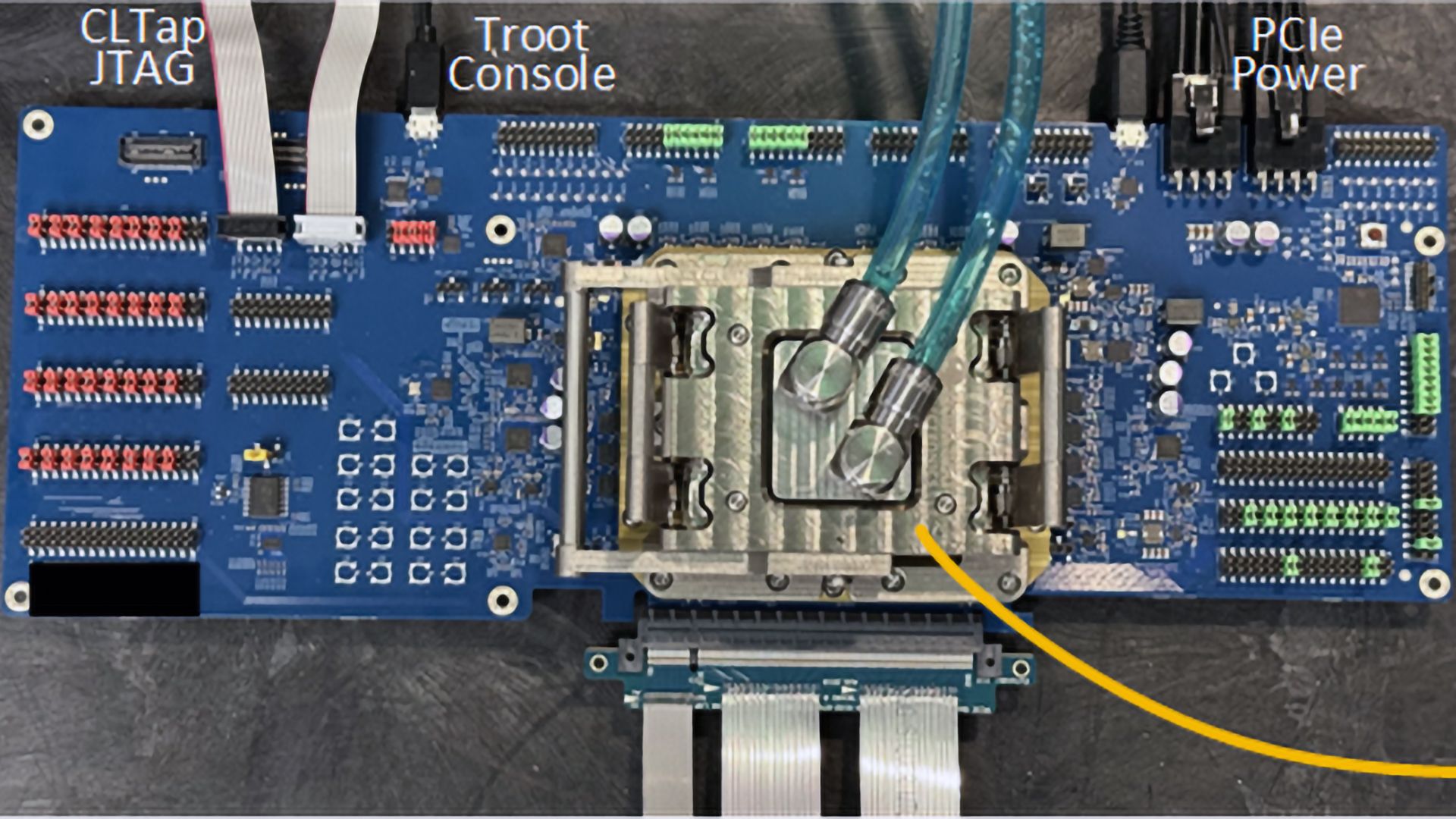
The accelerator is implemented as a PCIe card that sits alongside conventional x86 servers, currently requiring liquid cooling to sustain the 176 W TDP. It does not run general-purpose code and cannot boot an OS; it functions purely as an offload engine for FHE kernels.
Performance Analysis
Intel compared Heracles directly against a 24-core Intel Xeon W7-3455 “Sapphire Rapids” processor running at 2.5–4.8 GHz. The results are dramatic:
| Operation | Speedup vs Xeon W7-3455 | Absolute Time on Heracles | Notes |
|---|---|---|---|
| Key NTT transformation | 2,355× | 39 μs | Critical primitive |
| Operation 1–7 range | 1,074× – 5,547× | — | Seven representative FHE kernels |
| Voter ID matching example | ~1,071× | 14 μs (vs 15 ms on Xeon) | End-to-end application |
These speedups stem from the massive parallelism and specialized datapaths. A modern CPU core might process a single 32-bit limb per cycle with limited vector width, whereas Heracles processes 8,192 limbs simultaneously with custom butterfly hardware and optimized on-chip permutation networks.
Compared to prior academic and startup FHE accelerators (such as the asynchronous Galois Basalisc design), Heracles appears to be the first large-scale demonstration from a major semiconductor vendor using a synchronous, tiled, HBM-equipped architecture. While direct apples-to-apples comparisons with other silicon FHE projects are limited in public data, the 3–4 order-of-magnitude improvement over CPU baselines aligns with expectations for purpose-built accelerators.
Technical Implications
Heracles represents a pivotal step toward making FHE commercially viable. Privacy-preserving machine learning, encrypted database search, secure multi-party computation, and regulatory-compliant cloud analytics have all been theoretically possible but practically too slow. A 2,000–5,000× acceleration in core operations can reduce many workloads from minutes to seconds or from seconds to milliseconds, crossing the usability threshold for certain applications.
The PCIe card form factor allows incremental deployment: organizations can add Heracles cards to existing servers without replacing their entire compute fleet. This is crucial for adoption in regulated industries (finance, healthcare, government) where data sovereignty and confidentiality are paramount.
Longer term, success with Heracles could drive standardization of FHE primitives in software libraries (Microsoft SEAL, PALISADE, HElib) and encourage further co-design between cryptographers and hardware architects. It also signals that major vendors now view FHE as a strategic capability rather than a research curiosity.
Limitations and Trade-offs
Despite the impressive speedups, several caveats remain:
- Power and cooling: 176 W in a liquid-cooled PCIe card is manageable in data centers but precludes widespread edge or laptop deployment.
- Area and cost: At 197 mm² on Intel 3, the chip is relatively large. While pricing has not been disclosed, high-bandwidth memory and specialized logic suggest a premium product initially targeted at high-value use cases.
- Limited generality: Heracles cannot run general-purpose code. It is strictly an accelerator, requiring host CPU orchestration and data movement over PCIe, which adds latency.
- FHE overhead remains: Even with 2,000–5,000× acceleration, FHE is still slower than plaintext computation. Real-world applications must justify the cryptographic cost through privacy or compliance requirements.
- Bootstrapping cost: While the chip supports bootstrapping, this operation remains expensive and will likely dominate runtime for very deep circuits.
- Maturity: The design was demonstrated at ISSCC 2025; production availability, software stack completeness, and ecosystem support are not yet disclosed.
Expert Perspective
From a senior architect’s viewpoint, Heracles is significant not for raw TOPS but for proving that FHE can be accelerated by orders of magnitude through careful decomposition (32-bit limbs), massive SIMD, and domain-specific memory hierarchies. The choice of a tiled 8×8 mesh with dedicated permutation networks for automorphisms shows deep understanding of FHE dataflow.
The 32-bit slicing strategy is particularly clever: it converts the problem from “operate on gigantic integers” into “run thousands of parallel modular arithmetic lanes,” which maps beautifully to modern process technology. Intel’s ability to integrate 48 GB of HBM3 alongside the compute fabric also demonstrates mature packaging and power-delivery capabilities.
That said, the real test will be software usability. The accelerator’s value depends on seamless integration with high-level FHE compilers and libraries. If Intel can deliver a robust SDK that hides the tile scheduling, data staging, and bootstrapping orchestration, adoption could accelerate rapidly. Otherwise, Heracles risks remaining a sophisticated research prototype.
Technical FAQ
How does Heracles compare to a 24-core Sapphire Rapids Xeon on FHE workloads?
Across seven key FHE operations, Heracles delivers 1,074× to 5,547× speedup. The critical NTT primitive completes in 39 μs versus ~92 ms on the Xeon (2,355× improvement). A real application (encrypted voter ID matching) drops from 15 ms to 14 μs.
Is the architecture programmable for different FHE schemes and parameters?
Yes. Heracles supports BGV, BFV, and CKKS schemes with flexible parameter sets and security levels. The 32-bit lane design and configurable mesh routing allow software to tune for different polynomial degrees, modulus sizes, and multiplicative depths.
What are the memory and power characteristics?
The chip includes 48 GB HBM3 (two stacks), 64 MB on-chip scratchpad, and large per-tile register files. It operates at 1.2 GHz within a 176 W TDP and requires liquid cooling. Die size is 197 mm² on Intel 3 process.
How does this compare to other FHE accelerators such as Galois Basalisc?
Public data is limited, but Heracles uses a synchronous tiled approach with HBM3, while Basalisc employed asynchronous clocking domains. Intel’s design emphasizes massive 8192-way SIMD with 32-bit decomposition. Direct performance comparisons are not yet available, but Heracles is the first major-vendor demonstration at this scale.
References
- Intel ISSCC 2025 presentation (via IEEE Spectrum coverage)
- “Intel’s Heracles Chip Speeds Up FHE Computing,” IEEE Spectrum
- “Chips to Compute With Encrypted Data Are Coming,” IEEE Spectrum
- Additional reporting: Tom’s Hardware, Slashdot, Hacker News discussions