
MTIA Series: A Technical Deep Dive
Executive Summary
Meta has unveiled four generations of its Meta Training Inference Accelerator (MTIA) custom silicon developed in close partnership with Broadcom. The MTIA 300, 400, 450, and 500 chips target ranking & recommendation (R&R) and generative AI inference workloads. The family employs a chiplet-based, modular design with RISC-V vector cores, HBM memory, and a reusable chassis/rack/network fabric that enables a new chip roughly every six months. Meta claims the MTIA 400 already offers raw performance competitive with leading commercial products, while the MTIA 450 and 500 deliver substantially higher performance through aggressive HBM bandwidth scaling. Broadcom has stated Meta will deploy multiple gigawatts of these chips in 2027 and beyond. The announcement underscores Meta’s aggressive vertical integration strategy to reduce reliance on merchant silicon while supporting its massive AI inference demand.
Technical Architecture
The MTIA series follows a disaggregated, chiplet-first design philosophy that emphasizes modularity, yield optimization, and rapid iteration. All chips are built on a common reusable infrastructure at the chassis, rack, and network layers, allowing Meta to focus engineering effort on compute and memory while amortizing the cost of the surrounding platform.
-
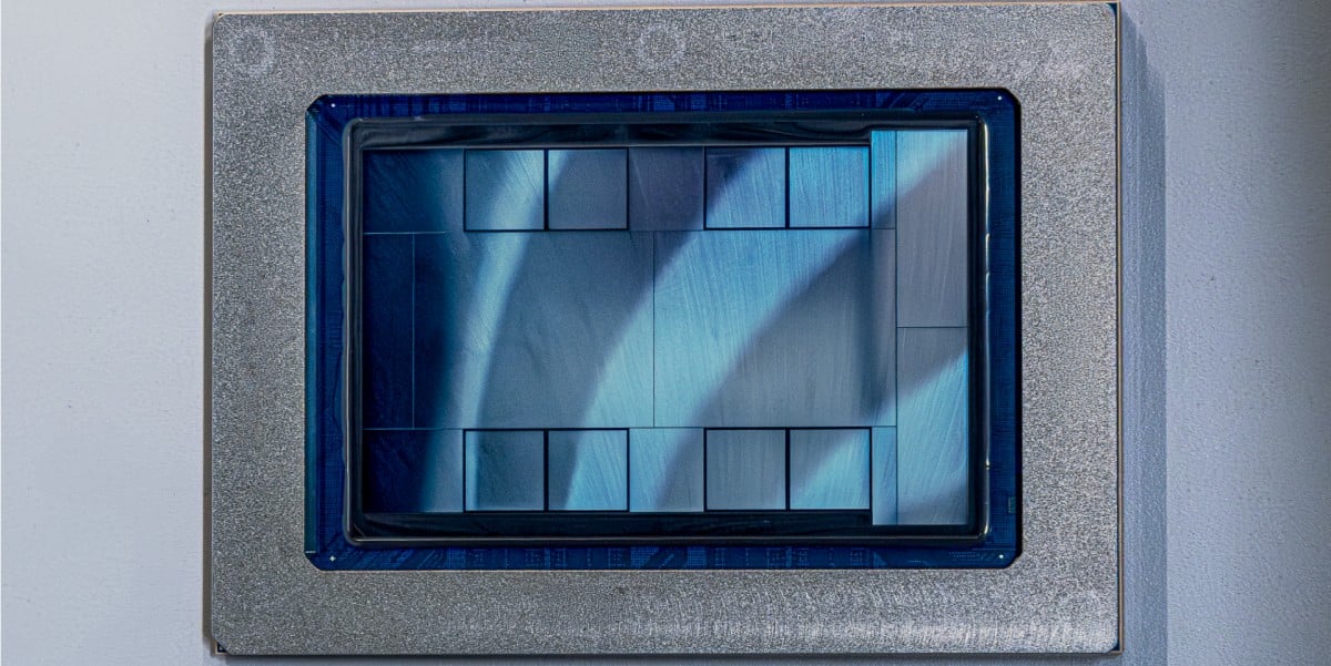
MTIA 300: The baseline communications-oriented accelerator optimized for ranking and recommendation workloads. It consists of one compute chiplet, two network chiplets, and multiple HBM stacks. The compute chiplet is organized as a grid of processing elements (PEs). To improve manufacturing yield, Meta includes redundant PEs. Each PE contains a pair of RISC-V vector cores, providing efficient SIMD-style processing for the sparse, irregular memory access patterns typical of recommendation models. The chip is already in production.
-
MTIA 400: An evolutionary step that adds support for generative AI models while retaining strong R&R performance. It doubles the compute resources to two compute chiplets. Meta states this is the first chip in the family whose “raw performance [is] competitive with leading commercial products.” A full rack contains 72 MTIA 400 devices connected via a switched backplane, forming a single large scale-up domain. This configuration allows efficient all-to-all communication within the rack without resorting to expensive off-rack networking for many workloads. The chip has completed testing and is “on the path to deploying” in Meta data centers.
-
MTIA 450: A GenAI-focused inference chip that doubles the HBM bandwidth relative to the MTIA 400. Meta claims this increase results in performance “much higher than that of existing leading commercial products” for inference. The chip is scheduled for mass deployment in early 2027.
-
MTIA 500: The most bandwidth-heavy member of the family. It increases HBM bandwidth by an additional 50% over the MTIA 450. The compute complex uses a 2×2 configuration of smaller compute chiplets (four chiplets total) surrounded by several HBM stacks, plus two network chiplets. An additional SoC chiplet provides PCIe connectivity to the host CPU and scale-out NICs. This heterogeneous chiplet approach allows Meta to optimize each die independently (compute, networking, I/O, memory controller). Mass deployment is planned for 2027.
All four chips share the same chassis, rack, and network infrastructure, dramatically reducing the non-recurring engineering (NRE) and operational complexity of rolling out successive generations. This “high velocity” design methodology reportedly enables Meta to ship a new chip roughly every six months.
The use of RISC-V vector cores is notable. By choosing an open ISA, Meta gains flexibility in instruction extensions, avoids licensing fees, and can customize the vector length and microarchitecture to its specific recommendation and transformer inference kernels. The grid-of-PEs organization suggests a spatially tiled architecture optimized for dataflow-style execution with local scratchpads or register files per PE.
Performance Analysis
Meta has not published conventional TOPS, TFLOPS, or power numbers in the announcement. Instead, it relies on qualitative and relative claims:
- MTIA 400: “raw performance competitive with leading commercial products” for both GenAI and R&R workloads.
- MTIA 450: “much higher” performance than leading commercial products, achieved primarily through doubled HBM bandwidth.
- MTIA 500: Further 50% HBM bandwidth uplift over the 450, targeting even more memory-bound inference scenarios.
The emphasis on HBM bandwidth as the primary performance lever is telling. Modern recommendation models and large transformer inference workloads are often memory-bandwidth bound rather than purely compute-bound. By aggressively scaling HBM bandwidth across the 400→450→500 lineage, Meta is optimizing for the actual bottlenecks seen in its production recommendation and Llama-family inference fleets.
Meta also highlights the scale of deployment. A single rack of MTIA 400 contains 72 accelerators under a switched backplane. When multiplied across “multiple gigawatts” of planned capacity in 2027, the fleet represents an enormous inference engine. Broadcom’s statement that Meta will install multiple gigawatts of these chips in 2027 and beyond implies tens or even hundreds of thousands of accelerators, given typical per-chip power envelopes in the 100–300 W range.
No independent benchmarks or head-to-head numbers against Nvidia H100, H200, B200, Google TPU v5/v6, or Amazon Inferentia/Trainium chips were provided. The absence of absolute performance figures or power-efficiency metrics (e.g., tokens per joule or queries per watt) makes direct comparison difficult. However, the repeated claim that the chips “outperform commercial silicon” suggests Meta believes it has achieved a meaningful total-cost-of-ownership (TCO) advantage when factoring in acquisition cost, power, and utilization on its specific workloads.
Technical Implications
The MTIA announcement represents a significant maturation of Meta’s custom silicon effort. Previously, the company had revealed early MTIA versions focused mainly on recommendation. The new family explicitly bridges recommendation and generative AI inference, reflecting the growing overlap between these workloads as Meta integrates Llama models into ranking, feed personalization, and content moderation.
By standardizing on a single chassis/rack/network fabric, Meta is applying hyperscaler playbook principles to silicon development itself. This approach lowers the marginal cost of each new chip generation and allows software teams to maintain a relatively stable target platform across multiple silicon revisions.
The partnership with Broadcom is strategically important. Broadcom brings expertise in high-speed SerDes, networking chiplets, and advanced packaging. The inclusion of dedicated network chiplets in every design indicates that scale-out and scale-up networking are first-class citizens rather than afterthoughts.
From an ecosystem perspective, Meta’s success with RISC-V vector cores and modular chiplets could encourage other hyperscalers to deepen their open-source ISA efforts. It also puts pressure on Nvidia, AMD, and Intel to either lower prices dramatically or deliver significantly better software ecosystems and performance-per-dollar on Meta’s specific mix of sparse recommendation and dense transformer inference.
Limitations and Trade-offs
Several limitations are evident from the announcement:
- Lack of transparency: No absolute performance numbers, power consumption, process node, die sizes, HBM capacities, or clock speeds were disclosed. This makes independent verification impossible.
- Workload specificity: The chips are heavily optimized for Meta’s internal recommendation and Llama-style inference. Performance on general-purpose AI tasks or training may be poor.
- Software maturity: While Meta has years of experience with its recommendation fleets, the newer GenAI support will require significant compiler, kernel, and framework work to reach high utilization.
- Yield and ramp risk: The use of multiple chiplets and redundant PEs acknowledges yield challenges, but complex 2×2 chiplet designs (MTIA 500) still carry integration and packaging risk.
- No training focus: Despite the “Training” in the MTIA name, all announced chips target inference. Meta continues to rely on commercial GPUs or other silicon for training.
Expert Perspective
Meta’s MTIA 300–500 series is one of the most ambitious custom AI silicon roadmaps publicly disclosed by a hyperscaler. The combination of rapid iteration (new chip every ~6 months), deep chiplet modularity, RISC-V vector cores, and aggressive HBM bandwidth scaling demonstrates a sophisticated understanding of both the hardware and workload characteristics.
The decision to standardize the entire rack infrastructure across three generations (400/450/500) is particularly clever. It transforms what is normally a high-risk, high-NRE activity into something closer to a software-like release cadence. If Meta can maintain software compatibility and achieve the claimed performance targets, it could materially reduce its AI infrastructure costs and lessen dependence on merchant GPU supply.
That said, the proof will be in the fleet-wide utilization and TCO numbers in 2027–2028. Until independent benchmarks or detailed performance data emerge, these claims remain directional. The emphasis on “outperforming commercial silicon” while providing almost no numbers is classic hyperscaler marketing. Still, the technical direction—more bandwidth, more modular chiplets, open ISA, and extreme deployment scale—is sound and likely to influence the broader AI silicon industry.
Technical FAQ
How does the MTIA series compare to Nvidia’s Hopper/Blackwell offerings on inference?
Meta claims MTIA 400 is already competitive and MTIA 450/500 are “much higher” performing than leading commercial products, primarily through HBM bandwidth. However, no tokens/second, latency, or power numbers were published, making precise comparison impossible. Nvidia retains advantages in software ecosystem, quantization tools, and general-purpose flexibility.
Is the MTIA platform backwards-compatible with previous generations?
The announcement states that MTIA 400, 450, and 500 all utilize the same chassis, rack, and network infrastructure. This implies software and mechanical compatibility at the rack level, though individual chiplet interfaces and host software stacks may require updates.
What process node and memory configuration are used?
Meta has not disclosed the process technology (expected to be TSMC 4 nm or 3 nm class given the timeline) nor exact HBM capacities or speeds. The progressive doubling and +50% HBM bandwidth increases are the only memory details provided.
Does Meta plan to open-source any part of the MTIA architecture?
No open-source plans were mentioned. While Meta has open-sourced some RISC-V work and PyTorch components, the MTIA chips themselves remain proprietary.
References
- Meta official technical blog post on custom silicon (March 2026)
- Broadcom statements on gigawatt-scale deployment
Sources
- Meta reveals custom AI chips it says beat Nvidia • The Register
- Meta Is Developing 4 New Chips to Power Its AI and Recommendation Systems | WIRED
- Meta debuts new AI silicon to power platform recommendations
- Meta Stock: Company Reveals Custom AI Chip Plans as Data Center Expansion Accelerates - CoinCentral
- Meta unveils four custom AI chips for data center growth By Investing.com