
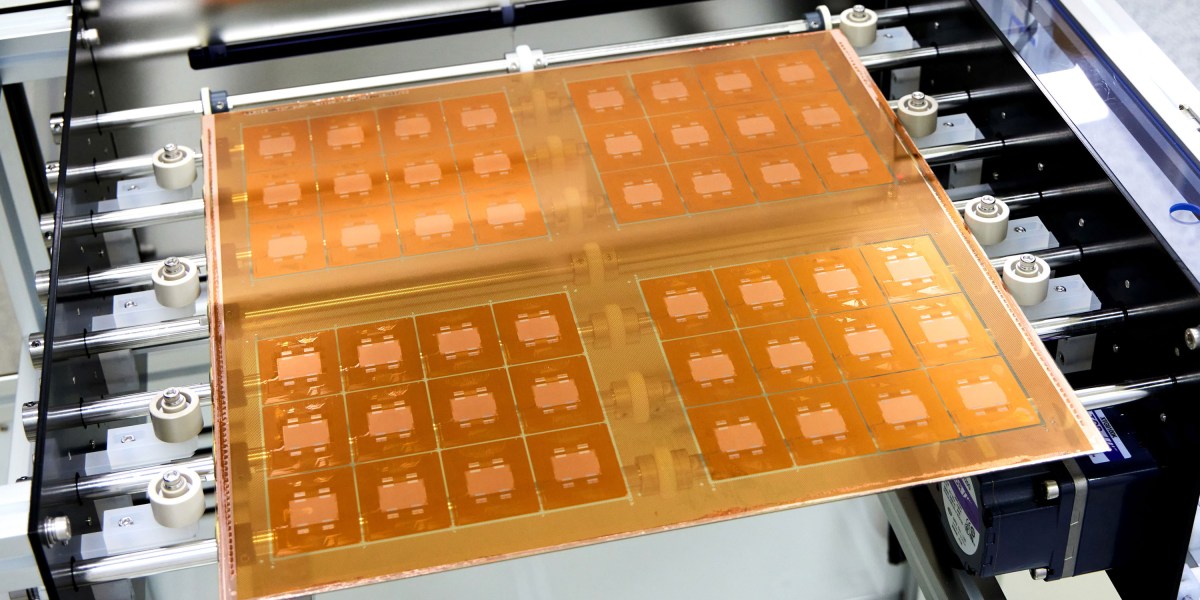
- What: Transition from organic substrates to glass-based chip packaging
- Who: Lead by Absolics (SKC), Intel, and Samsung, with support from AMD
- Key Performance: 10x increase in connection density and 50% more silicon capacity per package
- Timeline: Absolics commercial production starts in 2026; Samsung targeting 2028 transition
In a pivotal shift for the semiconductor industry, tech giants Intel, Samsung, and Absolics are moving to replace traditional organic materials with glass substrates to power the next generation of AI hardware. This transition aims to solve the "warpage" and thermal limitations currently bottlenecking high-performance computing, potentially delivering a massive leap in energy efficiency and processing density for data centers worldwide.
As AI workloads surge, the industry is hitting a "mechanical wall" with existing chip packaging technology. For decades, chips have relied on organic substrates made of fiberglass-reinforced epoxy. However, these materials are prone to shrinking, expanding, and physically warping under the intense heat generated by modern AI processors. According to Deepak Kulkarni, a senior fellow at AMD, these mechanical constraints are now a primary obstacle to the trajectory of high-performance computing.
Solving the "Warpage" Crisis
The move to glass is not merely aesthetic; it is a thermal necessity. Glass substrates remain stable at higher temperatures, allowing engineers to pack components more tightly without the risk of misalignment or premature failure caused by heat-induced distortion. This stability allows for the creation of denser interconnects—the copper-coated signal and power connections that link chips together.
Rahul Manepalli, vice president of advanced packaging at Intel, notes that glass’s thermal stability could allow for 10 times more connections per millimeter than organic substrates. This density enables designers to "stuff 50% more silicon chips into the same package area," significantly boosting the computational capability of a single unit while simultaneously improving cooling efficiency.
"The benefits of glass core substrates are undeniable," Manepalli stated, emphasizing that the material allows for more efficient routing of copper wires that deliver power, ultimately reducing the overall power consumption of the system.
The Global Race for Production
The transition is already moving from the laboratory to the factory floor. Absolics, a subsidiary of the South Korean firm SKC, has completed construction on a dedicated glass substrate facility in the United States. The company expects to begin commercial manufacturing this year, positioning itself as a first mover in the glass packaging market.
Intel is also accelerating its timeline. After a decade of research, Intel’s development teams are now reliably fabricating glass panels. In early 2025, the company successfully demonstrated a functional device with a glass core substrate booting the Windows operating system. This milestone proved that the technology is ready for real-world applications beyond theoretical benchmarks.
Samsung is following a similarly aggressive path. CEO Chang Duck-hyun has identified 2026 as the "defining year" for the commercialization of what he calls "dream substrates." Samsung reportedly plans to fully transition its AI chip manufacturing from silicon interposers to glass by 2028.
Overcoming Fragility
Despite the performance gains, working with glass presents unique manufacturing hurdles. The substrates are incredibly thin—ranging from 700 micrometers to 1.4 millimeters—making them highly susceptible to cracking or shattering during the assembly process.
To mitigate this, researchers at Intel and other firms have spent years developing specialized tools and integration materials to handle these fragile panels safely. While the current focus remains on high-end data center hardware where the performance-to-cost ratio justifies the investment, the industry expects that as manufacturing yields improve and production costs fall, the technology will eventually trickle down to consumer electronics, including laptops and mobile devices.
Impact on the AI Ecosystem
For AI developers and data center operators, the shift to glass represents a breakthrough in scalability. As models grow in complexity, the ability to pack more compute power into a smaller, more energy-efficient footprint is critical for maintaining the current pace of AI development.
"This changes how developers will scale AI models, removing the physical limits of heat that have held back chip density for years," says an industry analyst. The "Glass Revolution" effectively resets the clock on Moore's Law, providing the physical foundation upon which the next decade of AI breakthroughs will be built.
What’s Next
The industry is now entering a high-volume manufacturing (HVM) phase. While Absolics leads the immediate commercial charge in 2026, the broader ecosystem—including Chinese and South Korean suppliers—is rapidly investing in the glass packaging supply chain.
As these glass-core chips begin to enter data centers over the next 24 months, the focus will shift to monitoring long-term reliability in high-stress environments. If the technology holds up to the rigors of 24/7 AI processing, glass could become the standard foundation for all high-performance silicon by the end of the decade.